- 您现在的位置:买卖IC网 > Sheet目录317 > C8051F380-TB (Silicon Laboratories Inc)DEV KIT FOR C8051F38X
�� �
�
�C8051F380/1/2/3/4/5/6/7/C�
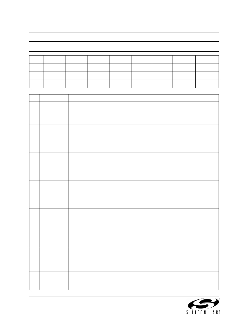
�SFR� Definition� 25.2.� SPI0CN:� SPI0� Control�
�Bit�
�7�
�6�
�5�
�4�
�3�
�2�
�1�
�0�
�Name�
�Type�
�SPIF�
�R/W�
�WCOL�
�R/W�
�MODF�
�R/W�
�RXOVRN�
�R/W�
�NSSMD[1:0]�
�R/W�
�TXBMT�
�R�
�SPIEN�
�R/W�
�Reset�
�0�
�0�
�0�
�0�
�0�
�1�
�1�
�0�
�SFR� Address� =� 0xF8;� SFR� Page� =� All� Pages;� Bit-Addressable�
�Bit� Name� Function�
�7�
�6�
�5�
�4�
�3:2�
�1�
�0�
�258�
�SPIF�
�WCOL�
�MODF�
�RXOVRN�
�NSSMD[1:0]�
�TXBMT�
�SPIEN�
�SPI0� Interrupt� Flag.�
�This� bit� is� set� to� logic� 1� by� hardware� at� the� end� of� a� data� transfer.� If� SPI� interrupts�
�are� enabled,� an� interrupt� will� be� generated.� This� bit� is� not� automatically� cleared� by�
�hardware,� and� must� be� cleared� by� software.�
�Write� Collision� Flag.�
�This� bit� is� set� to� logic� 1� if� a� write� to� SPI0DAT� is� attempted� when� TXBMT� is� 0.� When�
�this� occurs,� the� write� to� SPI0DAT� will� be� ignored,� and� the� transmit� buffer� will� not� be�
�written.� If� SPI� interrupts� are� enabled,� an� interrupt� will� be� generated.� This� bit� is� not�
�automatically� cleared� by� hardware,� and� must� be� cleared� by� software.�
�Mode� Fault� Flag.�
�This� bit� is� set� to� logic� 1� by� hardware� when� a� master� mode� collision� is� detected�
�(NSS� is� low,� MSTEN� =� 1,� and� NSSMD[1:0]� =� 01).� If� SPI� interrupts� are� enabled,� an�
�interrupt� will� be� generated.� This� bit� is� not� automatically� cleared� by� hardware,� and�
�must� be� cleared� by� software.�
�Receive� Overrun� Flag� (valid� in� slave� mode� only).�
�This� bit� is� set� to� logic� 1� by� hardware� when� the� receive� buffer� still� holds� unread� data�
�from� a� previous� transfer� and� the� last� bit� of� the� current� transfer� is� shifted� into� the�
�SPI0� shift� register.� If� SPI� interrupts� are� enabled,� an� interrupt� will� be� generated.� This�
�bit� is� not� automatically� cleared� by� hardware,� and� must� be� cleared� by� software.�
�Slave� Select� Mode.�
�Selects� between� the� following� NSS� operation� modes:�
�(See� Section� 25.2� and� Section� 25.3).�
�00:� 3-Wire� Slave� or� 3-Wire� Master� Mode.� NSS� signal� is� not� routed� to� a� port� pin.�
�01:� 4-Wire� Slave� or� Multi-Master� Mode� (Default).� NSS� is� an� input� to� the� device.�
�1x:� 4-Wire� Single-Master� Mode.� NSS� signal� is� mapped� as� an� output� from� the�
�device� and� will� assume� the� value� of� NSSMD0.�
�Transmit� Buffer� Empty.�
�This� bit� will� be� set� to� logic� 0� when� new� data� has� been� written� to� the� transmit� buffer.�
�When� data� in� the� transmit� buffer� is� transferred� to� the� SPI� shift� register,� this� bit� will�
�be� set� to� logic� 1,� indicating� that� it� is� safe� to� write� a� new� byte� to� the� transmit� buffer.�
�SPI0� Enable.�
�0:� SPI� disabled.�
�1:� SPI� enabled.�
�Rev.� 1.4�
�发布紧急采购,3分钟左右您将得到回复。
相关PDF资料
C8051F912DK
KIT DEV FOR C8051F91X/C8051F90X
C8051F930-TB
BOARD TARGET/PROTO W/C8051F930
C8051T610DB24
DAUGHTER BOARD T610 24QFN SOCKET
C8051T630DB20
BOARD SOCKET DAUGHTER 20-QFN
CAN-100
BOARD EVAL RS232 100QFP
CANADAPT28
KIT ADAPTER CANDEMOBOARD 28PLCC
CAT24AA01WI-GT3
IC EEPROM SERIAL 1KB I2C 8SOIC
CAT24AA02WI-G
IC EEPROM SERIAL 2KB I2C 8SOIC
相关代理商/技术参数
C8051F381
制造商:SILABS 制造商全称:SILABS 功能描述:USB DRIVER CUSTOMIZATION
C8051F381-GM
功能描述:8位微控制器 -MCU USB-64K-Flash
RoHS:否 制造商:Silicon Labs 核心:8051 处理器系列:C8051F39x 数据总线宽度:8 bit 最大时钟频率:50 MHz 程序存储器大小:16 KB 数据 RAM 大小:1 KB 片上 ADC:Yes 工作电源电压:1.8 V to 3.6 V 工作温度范围:- 40 C to + 105 C 封装 / 箱体:QFN-20 安装风格:SMD/SMT
C8051F381-GMR
功能描述:8位微控制器 -MCU USB-Flash-64k-ADC RoHS:否 制造商:Silicon Labs 核心:8051 处理器系列:C8051F39x 数据总线宽度:8 bit 最大时钟频率:50 MHz 程序存储器大小:16 KB 数据 RAM 大小:1 KB 片上 ADC:Yes 工作电源电压:1.8 V to 3.6 V 工作温度范围:- 40 C to + 105 C 封装 / 箱体:QFN-20 安装风格:SMD/SMT
C8051F381-GQ
功能描述:8位微控制器 -MCU USB-64K-Flash
RoHS:否 制造商:Silicon Labs 核心:8051 处理器系列:C8051F39x 数据总线宽度:8 bit 最大时钟频率:50 MHz 程序存储器大小:16 KB 数据 RAM 大小:1 KB 片上 ADC:Yes 工作电源电压:1.8 V to 3.6 V 工作温度范围:- 40 C to + 105 C 封装 / 箱体:QFN-20 安装风格:SMD/SMT
C8051F381-GQR
功能描述:8位微控制器 -MCU USB-Flash-64k-ADC RoHS:否 制造商:Silicon Labs 核心:8051 处理器系列:C8051F39x 数据总线宽度:8 bit 最大时钟频率:50 MHz 程序存储器大小:16 KB 数据 RAM 大小:1 KB 片上 ADC:Yes 工作电源电压:1.8 V to 3.6 V 工作温度范围:- 40 C to + 105 C 封装 / 箱体:QFN-20 安装风格:SMD/SMT
C8051F382
制造商:SILABS 制造商全称:SILABS 功能描述:USB DRIVER CUSTOMIZATION
C8051F382-GQ
功能描述:8位微控制器 -MCU USB-Flash-32k-ADC
RoHS:否 制造商:Silicon Labs 核心:8051 处理器系列:C8051F39x 数据总线宽度:8 bit 最大时钟频率:50 MHz 程序存储器大小:16 KB 数据 RAM 大小:1 KB 片上 ADC:Yes 工作电源电压:1.8 V to 3.6 V 工作温度范围:- 40 C to + 105 C 封装 / 箱体:QFN-20 安装风格:SMD/SMT
C8051F382-GQR
功能描述:8位微控制器 -MCU USB-Flash-32k-ADC RoHS:否 制造商:Silicon Labs 核心:8051 处理器系列:C8051F39x 数据总线宽度:8 bit 最大时钟频率:50 MHz 程序存储器大小:16 KB 数据 RAM 大小:1 KB 片上 ADC:Yes 工作电源电压:1.8 V to 3.6 V 工作温度范围:- 40 C to + 105 C 封装 / 箱体:QFN-20 安装风格:SMD/SMT